Heterojunction Interfacial Workfunction Internal Photoemission (HEIWIP) IR detectors
This project involves research on novel Heterojunction concepts, for
developing far infrared or terahertz detectors leading to potential
applications in important areas such as spectroscopy in chemistry and biology,
optical communication, plasma diagnostics, medical and biological imaging
systems, and astrophysics. Our group is developing 3-10 THz tailorable
solid state detectors operating at much higher temperatures than the traditional
4.2 K or below with the possibility of extending the frequency range to cover
1-10 THz a technologically important region for a wide range of applications.
Recent breakthroughs in THz generation has started bridging the gap existed
between terahertz frequencies and the frequencies above and below. However on
the THz detector development, extreme cooling capabilities are still a
requirement as in superconducting hot electron bolometers.
In order for the field to develop substantially both source and detectors should
develop at the same pace. Compatible material systems for both source and
detectors will make a rapid growth in the development. Primary goal of
this project will be to design and characterize THz detectors based on our
heterojunction
interfacial workfunction internal photoemission (HEIWIP) concept and optimize
the devices for various frequency (wavelength) ranges. The work will include
both experimental and theoretical effort studying the role of device parameters
on the performance including the doping, barrier parameters, layer thickness,
resonance cavity effects and dark current issues. HEIWIP
far-infrared detectors where the workfunction is primarily due to an
AlGaAs layer next to a doped GaAs (emitter) layer has some similarities with our
previous work on Homojunction interfacial workfunction internal photoemission
detectors (HIWIP). However, the novel HEIWIP concept avoids the high dark
current and defects associated with heavy doping and related space charge
issues. In the HEWIP setectors the emitters are doped to a sufficiently high
level so that the carriers form a 3-dimensional distribution in the emitters and
detection is by free-carrier absorption just as in the case of HIWIPs. However
this will still be very much below the concentrations needed for HIWIP
detectors. The barriers have a low Al fraction so that the workfunction
(difference between the barrier conduction band and the 3-D Fermi level in the
emitters) will be small allowing operation at FIR wavelengths. By adjusting the
Al fraction (and to a lesser extent the emitter doping density)
cutoff wavelength can be tailored to any desired wavelength. The doping in
the emitters of the GaAs/AlGaAs structures should be kept low to
reduce the dark current to levels comparable or lower than those of QWIPs
(quantum well infrared photodetectors), while the use of free-carrier absorption
in the
emitter regions rather than the intersubband transition used in QWIPs will give
the high responsivity observed in HIWIPs. Increasing the doping in the emitter
region will increase the absorption in the emitters but will also increase the
dark current. The optimum doping of the emitter regions will have to be
determined by balancing the dark current and absorption quantum efficiency in
the emitter regions. Thus HEIWIPs can combine the best properties of the QWIP
and HIWIP detectors leading to improved operation.
Return to
Dr. Perera's Homepage
Return to
Physics & Astronomy Homepage
Multi
and Dual Band Infrared detectors
Detecting electromagnetic radiation in two or more spectral bands with a single detector element has many applications in many areas such as defense and astronomy. Advantages of multi band photo detectors include less space requirements, low power requirements, and simple read out circuitry. Furthermore, simultaneous measurements of different spectral bands with a single detector element will fulfill many badly needed requirements in sensors and imagine industries. We currently work on ultraviolet-infrared (UV-IR) dual band detectors and infrared multi band detectors. GaN based materials are being investigated to obtained high performance UV-IR dual band detectors. Different types of UV-IR detector designs and different electrical contact layouts are being investigated for simultaneous UV and IR spectral measurements. Quantum dot (QD), quantum dots in a well (QDWELL), and tunneling quantum dot infrared photo detectors (TQDIP) based on GaAs/InAs structures are studied for multi band IR detectors. We have strong collaborations with research institutes such as Georgia Institute of Technology (Prof. I. Ferguson), University of Michigan (Prof. P. Bhattacharya), University of New Mexico (Dr. S. Krishna) and NRC Canada (Dr. H. C. Liu). This project offers young researchers excellent experimental experiences as well as basic and cutting edge device physics knowledge.
Return to
Dr. Perera's Homepage
Return to
Physics & Astronomy Homepage
Uncooled Infrared
detectors
The room temperature detection
of infrared radiation is becoming important for a wide range of applications in
the civilian, industrial, medical, astronomy, and military sectors. Excitation
mechanism between
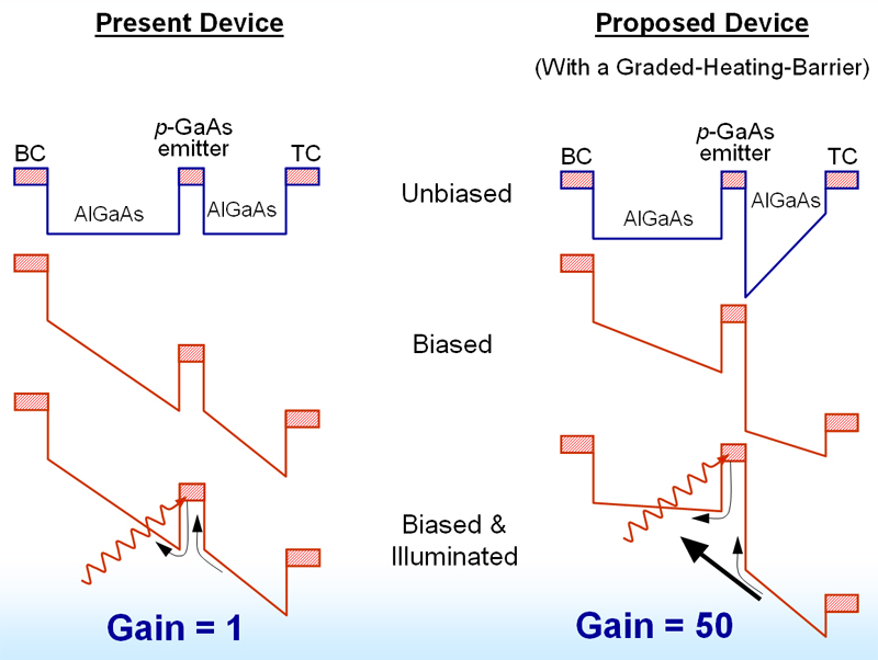
The band diagram showing the difference between regular barrier and the proposed graded-heating-barrier. Both detector structures consist of p-GaAs emitter and AlGaAs barrier. Here BC and TC indicate the bottom and top contact layers. (a) Detector structure with regular barriers under unbiased, biased, and illuminated conditions with no gain. The arrows indicate the hopping mode carrier transport mechanism. (b) Detector structure with graded heating barrier under unbiased, biased, and illuminated conditions. Here most of carriers transport over the well giving enhanced gain.
Return to
Dr. Perera's Homepage
Return to
Physics & Astronomy Homepage
Quantum-dot
Infrared detectors
InAs/GaAs, InGaAs/GaAs, and InAs/InGaAs
based quantum dot(QD) detectors, quantum dots in a well (QDWELL) detectors, and
tunneling quantum dots infrared photo detectors (T-QDIP) are studied for multi
color detection capabilities at higher temperatures. We have successfully
demonstrated multi color detection capabilities in MIR/FIR ranges at higher
temperatures using QDWELs and T-QDIPs device structures. Using tunneling
barriers, low dark currents and higher detectivities have been achieved. In
addition, polarization sensitive and tunable multi spectral photo detectors
based on QD structures are being investigated. These polarization sensitive and
tunable multi spectral detectors are useful in defense, astronomy, medical, and
pharmaceutical industry. The possibilities of using QD based devices as
terahertz detectors are also being investigated.
This work is carried out in collaborations with
Return to
Dr. Perera's Homepage
Return to
Physics & Astronomy Homepage
Homojunction Interfacial Workfunction Internal Photoemission (HIWIP) IR detectors
Multilayer formats were explored for detection in the far infrared (FIR). It was demonstrated that internal photoemission involves a work-function interface barrier (determining the long wave cutoff), and requires high doping (approaching the metal-insulator transition) of the absorber/emitter layer. For high quantum efficiency, the focus is on thin, high-quality MBE layers in Multi Quantum Well (MQW) formats. For optimum absorption, depletion and carrier diffusion, doping levels only sufficiently high to extend the IR cutoff to the desired range (through impurity-band broadening) are emphasized. In collaboration with scientists at other universities and national laboratories, the operation mechanisms and the device physics of a variety of Si, GaAs and MQW detector structures will be analyzed and will be experimentally demonstrated. A body of detailed modeling and experimental data has been published from which selected promising device formats can now be developed and optimized for early practical application. The key to achieving these objectives depends upon further critical experiments on single and multi-layer structures in which the emitter/collector and p- or n- drift layers are both epitaxially grown. Our goal is to clearly understand the influence of doping and dimensional parameters, and of bias conditions, on detector and array spectral response, dark current and NE delta(T) performance. Approaches will be examined for suppressing dark current, by narrowing spectral response, by blocking impurity band conduction (for lower absorber doping samples), by configuring energy-selective tunneling barriers (especially in the case of GaAs/AlGaAs MQW structures), and by employing guard-ring or surface passivation procedures. This barrier effort will be conducted in conjunction with MBE experts at Cornell ,NRC and UCLA
Return to
Dr. Perera's Homepage
Return to
Physics & Astronomy Homepage
Dye
Sensitized Semiconductor Nanostructure
Dye-sensitized IR detectors, which are low cost and work at room temperature, are developed under this project. A structure consisting of a dye layer sandwiched between two semiconductor layers can be used as near infrared photo detectors. The dye layer acts as the IR absorber and photoexcited electrons in the dye layer are injected to the adjacent semiconductor resulting in a photocurrent. We study different combinations of IR sensitive dyes and metal oxide semiconductors such as TiO2, SnO2, ZnO, CuSCN, and CuI to optimize the performance of these IR detectors. This project is carried out in collaboration with IFS-Sri Lanka (Prof. K. Tennakone).
Return to
Dr. Perera's Homepage
Return to
Physics & Astronomy Homepage
Semiconductor
Materials Properties
Material properties play a major
role in designing opto-electronic devices. Optical properties of semiconductor
thinfilms are been investigated in order to design novel opto-electronic devices
and to optimize existing opto-electronic devices. We have facilities to carry
out reflection and transmission measurements covering UV range to far infrared
range using either a monochromator (from UV to NIR) or a FTIR (from NIR to FIR).
IR dielectric function modeling and IR reflection (transmission) fittings
are also carried out to study the materials properties such as Phonon
properties, high frequency and static dielectric constants, refractive index,
absorption coefficient, etc. Optical properties of various materials such as
AlGaAs, AlGaN, GaN, GaMnN, GaSb, and InN thinfilms have been studied.
These results are readily used for designing and optimizing IR detectors.
Facilities are available to carry out photoluminescence measurements from 4.2 to
300 K to study fundamental band gap energy and impurities in materials.
Photoluminescence measurements are carried out using a custom � built
system using a FTIR spectrometer, which has the capability of averaging of
several hundreds of spectra in a relatively short time.
Major instruments available for optical characterizations include two
Perking Elmer FTIR systems, a high power Argon laser system, a CO2
laser system, and two fully automated monochromator system. Here, we work with
our colleges at GSU (Dr. N. Dietz) and other research institutes as NRC-Canada
(Dr. H. C. Liu) , Soreq NRC-
Return to
Dr. Perera's Homepage
Return to
Physics & Astronomy Homepage
Physics of QWIPS
Extending on our recent analysis of transient modes of detection and of space-charge distribution in multi-layer GaAs/AlGaAs structures, studies on the frequency and bias dependence of sensor response will be continued, with the aim of establishing optimum operation parameters. These efforts will also have an important bearing on the potential for using such multi-layer devices as IR sensors or in the heterodyne mode. In pursuing these studies, we will attempt (though the interaction with other scientists) to reconcile the detector performance goals with desired array operation modes and geometry, and with system design requirements.
Return to
Dr. Perera's Homepage
Return to
Physics & Astronomy Homepage
Infrared Emission
We have studied Infrared emission using intersubband transitions in GaAs/AlGaAs multi-quantum well structures. Even for energies higher than the optical phonon values, the photon emission process which is limited by the competition from nonradiative relaxations seems probable when the relative efficiencies are compared. The efficiency of 10 µm emission is comparable to that of 110 µm, and could be even improved for shorter wavelengths. Our results from a two level (in the well) and a three level structure show evidence for LWIR emission in the ranges of 8-11.5 µm and 9-14 µm respectively. More recent work of (Formerly known as AT & T Bell laboratories) Lucent Technologies group headed By Dr. F. Capasso, realizing Semiconductor IR Lasers confirms our initial predictions. More recently, in Collaboration with our Korean colleagues, We have worked on improving the understanding of resonant tunneling times, from the spacing of the energy doublets arising at resonance. This correct estimation of energy level and the resonant tunneling time can be the starting point of the optimization of quantum cascade lasers reported by the Bell Labs group.
Return to
Dr. Perera's Homepage
Return to
Physics & Astronomy Homepage
Pulsing and Nonlinear Dynamics
We have studied the mechanisms of spontaneous pulsing in semiconductor structures. This has led us to realizing novel infrared detectors which does not need any preamplifiers. The fluctuations in the interpulse time intervals have created an interest in nonlinear dynamics. These resulted in studies of bifurcation, Chaos and route to periodicities. An iterative map was derived from the device equations for a silicon p+-n-n+ diode, which emulates a biological neuron. This map is extended to a coupled neuron circuit which could be used as a single channel of a parallel asynchronous processor. The extended map output is studied under different driving conditions, showing fixed points (both stable and unstable) and limit cycles. A comparison of modeling outputs with the experimental outputs show a Hopf bifurcation. Also observed are the periodic and chaotic responses of a network corresponding to recognition or lack of recognition of IR signals.
Return to
Dr. Perera's Homepage
Return to
Physics & Astronomy Homepage
Semiconductor Neurons
We have developed an approach based on silicon p-i-n devices to emulate neural networks. The approach emphasizes wetware emulation as a guide to neural network hardware development providing legitimate constraints on neural network implementation which would favor biologically realistic models. We have shown that a realistic model can be built with features such as analog-digital mixed character, systems as originally described by von Neumann, spiketrain generation (from two-terminal integrate-and-fire devices) and nonlinear dynamics concepts of network activity suggested by the work of Freeman et al. The spiketrains are used as physical representations of time series, and parametrically modulated iterative maps as time series encoding functions, neurons as parametrically modulated time series transceivers, pulse height discrimination as a means of noise rejection. The hardware is used to show the transient signal sensing as in the case of a horseshoe crab eye. An iterative map is developed for a single channel of a proposed processor. The output of the model is compared with the experimental outputs. Device parameters are identified with the iterative map parameters. We are in the process of developing Multiple Quantum Well Structures which can be used as artificial Neurons at much higher temperatures than the p-i-n structures.
Return to
Dr. Perera's Homepage
Return to
Physics & Astronomy Homepage